
Analog Devices Explores Gallium Nitride Innovation
Oct 02 2025
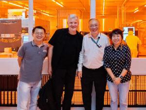
The National Semiconductor Translation and Innovation Centre for Gallium Nitride (NSTIC GaN) welcomed the team from Analog Devices (ADI) for a knowledge exchange focused on the advancement of RF and high-frequency technologies. The session provided valuable discussions on how Gallium Nitride innovation continues to drive performance, efficiency, and communication capabilities in next-generation systems. NSTIC (GaN) also shared its role in supporting semiconductor research and development that contributes to Singapore’s growing position as a hub for deep-tech innovation.
Overview of the Visit
The visit by Analog Devices provided an opportunity for both teams to exchange views on Gallium Nitride’s role in emerging communication and power technologies. Representatives from ADI included:
-
Zoran Zvonar, Fellow, ADI Garage
-
Laura Yan, Senior Director of Marketing
-
Ho Vui Min, Senior Manager, Analog Design Engineering
-
Mark Foo, Senior Sales Manager, APAC (excluding India)
Discussions covered GaN’s characteristics as a wide bandgap material and its relevance to improving device performance, power efficiency, and integration in radio frequency applications.
Focus on Gallium Nitride and RF Technologies
Gallium Nitride is recognised for its wide bandgap properties that allow high breakdown voltage, efficiency, and thermal stability. These characteristics make it suitable for high-frequency and high-power devices used in RF communications, radar, and industrial systems.
During the session, NSTIC (GaN) researchers shared an overview of ongoing R&D activities and infrastructure supporting GaN device development. The exchange also touched on the translation of research outcomes into practical implementations relevant to future communication systems.
Singapore’s Semiconductor Research Landscape
NSTIC (GaN) serves as part of Singapore’s wider research ecosystem supporting semiconductor technology and advanced materials development. Visits such as this reflect ongoing engagement between research institutions and industry representatives that contribute to the exchange of technical perspectives within the community.
These interactions offer opportunities for mutual understanding of research directions, practical applications, and shared challenges faced across the semiconductor value chain.
Final Thoughts
NSTIC (GaN) expresses its appreciation to the Analog Devices delegation for the insightful discussions and knowledge sharing during their visit. The session provided a platform for mutual learning and technical exchange in the field of Gallium Nitride semiconductor technology.