Empowering the Future of GaN Technologies
NSTIC (GaN) combines cutting-edge tools, seamless process integration, and future-ready platforms to deliver precision and performance in Gallium Nitride (GaN) technologies. Our advanced infrastructure supports applications across 5G networks, high-frequency communication, and next-generation devices, meeting the demands of evolving industries. With innovations reaching up to 140 GHz, we empower breakthroughs for today and tomorrow.

Cutting-Edge Tools
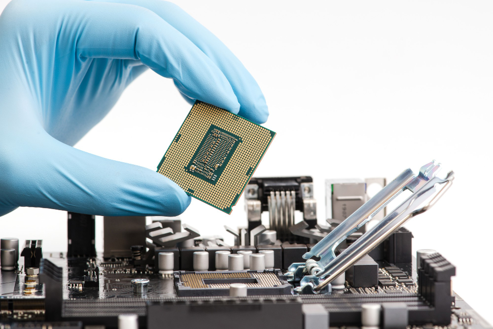
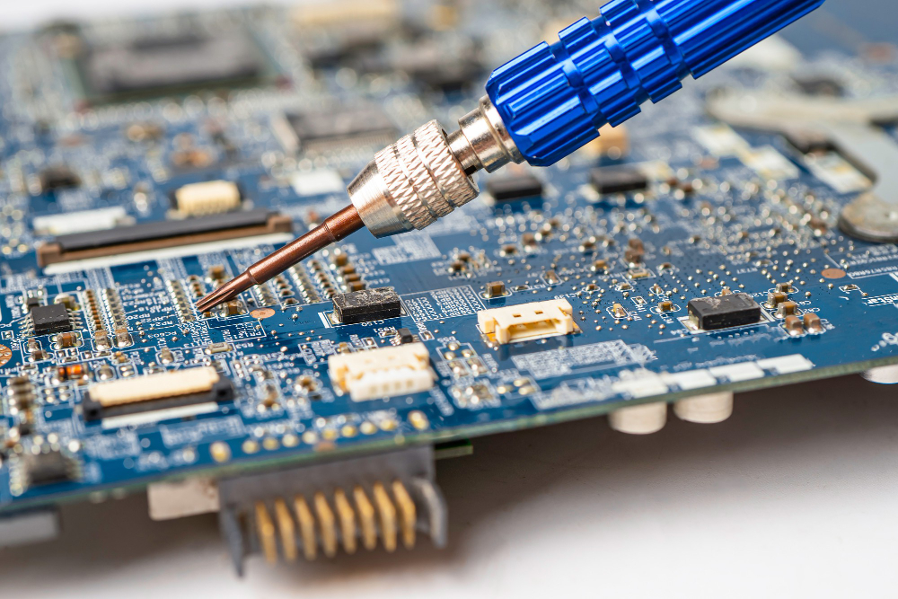
NSTIC (GaN) utilises state-of-the-art tools such as Electron Beam Lithography (EBL) and Atomic Layer Deposition (ALD/ALE) to achieve nanometre-scale precision in fabrication processes. Our advanced inspection systems ensure exceptional reliability and low defect rates, delivering the precision needed for high-performance applications across industries.

Full Process Integration
Seamless integration of GaN-on-SiC and GaN-on-Si fabrication lines enables NSTIC (GaN) to support diverse industry demands, from high-frequency RF/mmWave applications powering 5G and 6G networks to low-voltage, high-efficiency solutions for mobile devices and advanced instrumentation. This integrated approach ensures scalability and performance without compromise.

Future-Ready Platforms
NSTIC (GaN)’s platforms are built for next-generation technologies, featuring gate-lengths smaller than 0.25μm to achieve higher frequencies up to 140 GHz. These capabilities unlock emerging applications in mmWave satellite communications, automotive radar systems, advanced instrumentation, and critical defence solutions, positioning NSTIC (GaN) at the forefront of innovation.
Precision, Scalability, and Future-Ready Innovations


6” Gold-based Line
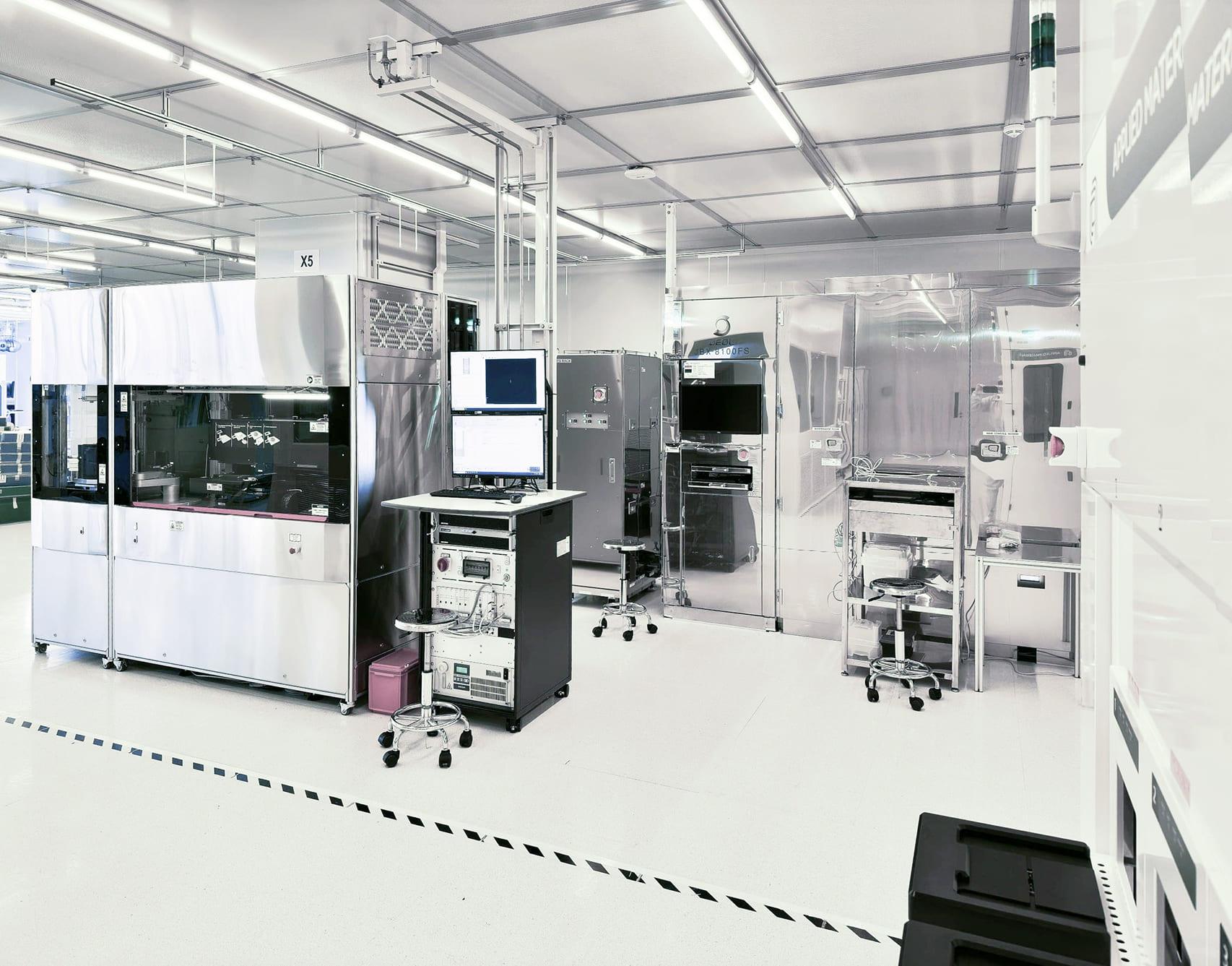
6” GaN-on-SiC production in 700m² Class 100 Cleanroom for non-CMOS processes
- Processing Tools:
-
-
- Electron Beam Lithography – capable of up to 40nm resolution
- Laser Writer – enabling maskless lithography
- Atomic Layer Etcher – enabling precise material removal
- Ebeam Evaporator – capable of both conformal and non-conformal deposition
- Physical Vapour Deposition (PVD) – enabling conformal Gold(Au) seed deposition in through-silicon via (TSV) structures
- Inductive Coupled Plasma-Chemical Vapour Deposition (ICP-CVD) – enabling Si-rich dielectric layers at low temperatures
- Electroless Plating System – enabling cheaper and efficient deposition of thick Nickel(Ni), Gold (Au) layers in TSV structures
-
-
- Inspection/Characterisation:
-
-
- Automatic Optical Inspection – providing prompt inline wafer defects detection
- Critical Dimension (CD)-Scanning Electron Microscope(SEM) – providing real-time read outs of critical dimension
- 3D Viewing Microscope – real-time inline process monitoring
- In-line Automatic Wafer Prober – inline device testing
-
-
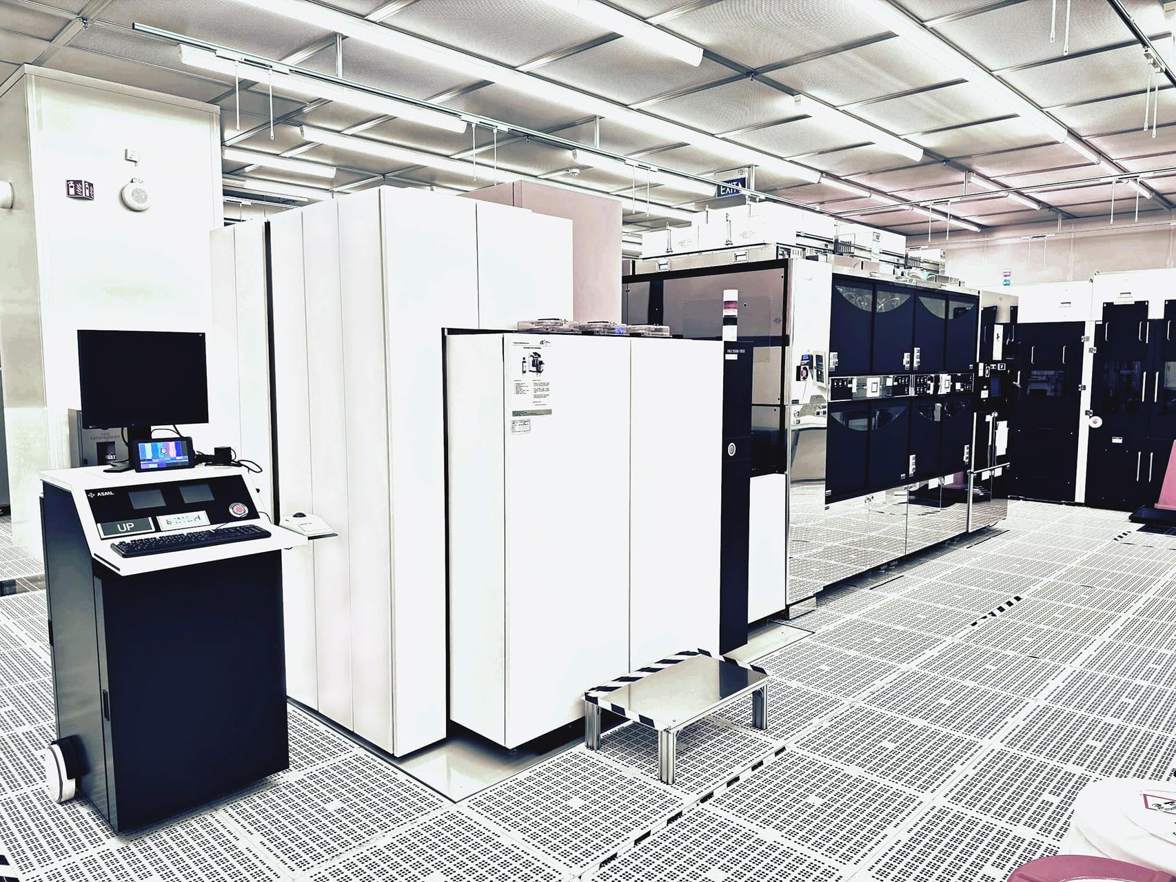
8” CMOS-compatible Line
8” GaN-on-Si (ESD certified) production in 1,200m², Class 100 Cleanroom for CMOS-compatible processes
- Processing Tools:
-
-
- Deep-ultraviolet(DUV) Scanner – capable of up to 250nm resolution
- Physical Vapour Deposition (PVD) – enabling thin, conformal metal layer deposition
- Plasma-enhanced Chemical Vapour Deposition (PECVD) – enabling high-quality dielectric layers at low temperatures
- Metal and Non-Metal Wet Benches – provide a wide range of cleaning and wet etching solutions
-
-
- Inspection/Characterisation:
-
-
- Defects Review(DR)- Scanning Electron Microscope(SEM) – real-time process defects scan and review
- Critical Dimension (CD)- Scanning Electron Microscope(SEM) – providing real-time read outs of critical dimension
-
-
Characterisation and Qualification Lab
ESD certified test laboratory (250m²)
- Electrical
-
-
- 8” wafer temperature test from -60 to 300 °C
- Pulsed-IV measurement with pulse width down to 500 ns
- CW/Pulsed-based RF scattering parameter up to 65 GHz
- Single/Two tone active load pull up to 20 W
- Modulation-based load pull test with ACPR and EVM
-
-
- Reliability
-
-
- 64-channel DC HTOL test
- 32-channel RF HTOL test from 2 to 18 GHz
- Max. 100 W DC power dissipation with Tₐ up to 100°C per channel
- RF power stimulation up to 1 W per channel
-
-
Delivering Precision and Innovation in GaN Technologies
At NSTIC (GaN), we bridge research and manufacturing excellence to deliver high-performance solutions in Gallium Nitride (GaN) technologies. Our advanced facilities empower industries to develop reliable, scalable, and future-ready applications for communication systems, precision devices, and next-generation electronics.
Innovative GaN Solutions
Advanced Inspection & Quality