
Recent Progress and Task of GaN Materials and Devices for Power Applications
Nov 20 2024
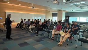
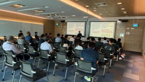
On 19 November 2024, NSTIC (GaN) was honoured to host Dr Yohei Otoki for an insightful seminar focused on the recent progress and challenges in gallium nitride semiconductor materials and devices for power applications. The event brought together researchers and industry professionals to discuss new advancements in GaN-based devices and their growing role in modern electronics.
Advancements in GaN Materials and Devices
During the session, Dr Otoki shared key developments in the mass production of GaN-HEMTs for radar systems and introduced new materials such as InAlGaN. These innovations are designed to meet the demanding requirements of 6G communications and satellite technologies. As a result, GaN continues to pave the way for greater efficiency, reliability, and scalability in high-frequency and power applications.
Furthermore, Dr Otoki highlighted how gallium nitride semiconductor devices are driving change across multiple sectors. Their ability to handle higher voltages and frequencies makes them essential for next-generation energy systems and compact, high-performance electronics.
Exploring Power-Switching Innovations
In addition, Dr Otoki presented breakthroughs in power-switching devices, including GaN-HEMTs on silicon and vertical GaN-MOS structures. These technologies are setting new standards in performance and energy efficiency. They also demonstrate how GaN can outperform conventional materials in both speed and thermal management, which is critical for emerging smart energy and communication systems.
The seminar emphasised that continued research into GaN epitaxy, reliability testing, and device architecture will be key to scaling power applications. With GaN’s wide bandgap and high electron mobility, these devices can deliver superior performance while consuming less energy—an essential step toward sustainability in advanced electronics.
Insights from Dr Yohei Otoki
Dr Otoki has made significant contributions to gallium nitride semiconductor research over the past four decades. He graduated from Kyushu University and began his career at Hitachi Cable in 1980. Since then, he has focused on the growth and characterisation of compound semiconductor crystals such as GaAs, GaN, and diamond.
In 1994, he earned his Ph.D. from Kyushu University, specialising in semi-insulating GaAs crystals for high-frequency devices. Between 2008 and 2011, he worked in Silicon Valley, gaining experience in engineering and business development. Dr Otoki also served as conference chair of CS-MANTECH 2011 and continues to contribute actively to international semiconductor forums.
His lifelong dedication to advancing GaN technologies has helped improve device efficiency, yield, and manufacturability. Through his leadership, the gallium nitride semiconductor industry continues to evolve toward higher performance and commercial scalability.
Looking Ahead
Dr Otoki’s seminar provided an in-depth exploration of both the progress and the challenges facing GaN materials today. His discussion on mass-production techniques, new material systems like InAlGaN, and high-efficiency device architectures reinforced the transformative role of GaN in power electronics and high-frequency technologies.
Moving forward, NSTIC (GaN) remains committed to supporting research and development in GaN materials and devices. By connecting scientific discovery with real-world application, we aim to help shape the future of power systems, communication networks, and sustainable technologies.