
A New Chapter in Singapore’s Semiconductor Story: Official Opening of NSTIC (GaN)
Jun 27 2025
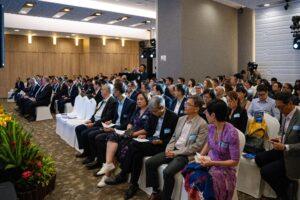
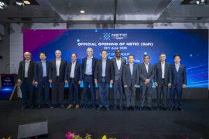
On 26 June 2025, Singapore marked a defining moment in its deep-tech journey with the official launch of the National Semiconductor Translation and Innovation Centre for Gallium Nitride (NSTIC GaN). More than an inauguration, the event signified the nation’s growing leadership in next-generation semiconductor research and innovation.
Jointly established by A*STAR, DSO National Laboratories, and Nanyang Technological University (NTU), NSTIC (GaN) brings together infrastructure, talent, and translational R&D to advance Gallium Nitride technologies for applications such as 5G, satellite communications, power electronics, and smart mobility. The launch represents a significant stride forward for the semiconductor industry in Singapore.
Messages That Set the Tone
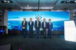
The ceremony was officiated by Dr Tan See Leng, Minister-in-Charge of Energy and Science & Technology. Distinguished guests in attendance included:
-
Mr Cheong Chee Hoo, CEO, DSO National Laboratories and Chair, NSTIC (GaN) Steering Committee
-
Professor Yeo Yee Chia, Deputy Chief Executive (Innovation & Enterprise), A*STAR
-
Professor Lam Khin Yong, Vice President (Industry), NTU
-
Professor Ng Geok Ing, Executive Director, NSTIC (GaN)
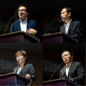
In his opening remarks, Mr Cheong highlighted NSTIC (GaN)’s role as a national platform bridging foundational research with industry-aligned applications. Dr Tan’s keynote reinforced the importance of GaN technologies in shaping Singapore’s future infrastructure—from communications and satellite systems to electric mobility. His message reflected a broader national ambition: to build a science-driven, innovation-led semiconductor industry in Singapore that delivers global impact.
A Declaration of Partnerships
The launch also underscored NSTIC (GaN)’s collaborative spirit through the announcement of several formal partnerships with:
-
Waferlead
-
ST Engineering
-
Oxford Instruments
-
Rohde & Schwarz
-
SHINE (NUS)
-
Incize
These partners represent a cross-section of expertise, from advanced RF testing and MMIC development to materials characterisation and thermal modelling. Presentations from partner organisations offered guests a preview of ongoing joint initiatives, signalling strong momentum beyond the launch itself.
A Closer Look Behind the Scenes
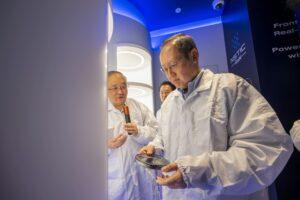
During his visit, Dr Tan toured NSTIC (GaN)’s facilities, including its cleanroom, process development areas, and prototyping laboratories. The walkthrough provided a first-hand look at the national infrastructure supporting GaN materials research, device fabrication, and systems integration.
The facility tour reinforced how national platforms and ecosystem partnerships can accelerate deep-tech innovation and strengthen local capabilities. The day concluded with a networking session that connected representatives from government, academia, and industry, reflecting the spirit of collaboration driving the semiconductor industry in Singapore.
A New Chapter Begins
The official opening of NSTIC (GaN) represents more than a ceremonial milestone—it marks the beginning of a new era in Singapore’s semiconductor journey. The centre will serve as a catalyst for technological breakthroughs, commercial partnerships, and global collaboration.
NSTIC (GaN) expresses its appreciation to Dr Tan See Leng, all partners, speakers, and guests for being part of this milestone event. The relationships forged during the launch are already helping to shape the next chapter of Singapore’s innovation landscape.
What’s Next
NSTIC (GaN) now enters a phase of execution and growth. We are excited to deepen collaborations, strengthen our ecosystem, and continue advancing GaN technologies that drive national innovation priorities.
Thank you for being part of this journey. The future of semiconductors starts here.