
NSTIC (GaN) Highlights Scalable GaN-on-Si Milestones at 10th IEEE EDTM in Penang
Mar 06 2026
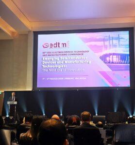
Our team recently participated in the 10th IEEE Electron Devices Technology and Manufacturing (EDTM) Conference in Penang, Malaysia. This annual forum serves as a vital platform for sharing semiconductor progress. During the conference, our team focused on the industrial readiness of GaN-on-Si technology.
Optimising Low-Voltage GaN-on-Si for Next-Generation Devices
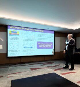
To begin the sessions, Prof. Ng Geok Ing shared joint NSTIC(GaN) – NTU research. This presentation focused on the optimisation of GaN-on-Si HEMTs for low-voltage operations.
As a result of this work, we are uncovering new possibilities for power-sensitive electronics. This versatility suggests that our platform could eventually support a wide range of devices. For instance, there is clear potential for applications in both 5V mobile handsets and high-power infrastructure.
Industrialising GaN: 200 mm Manufacturing Readiness for FR3
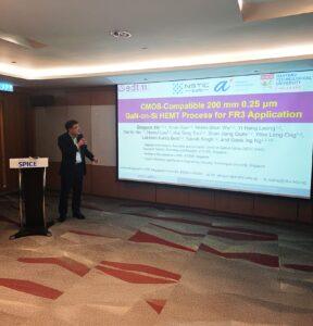
Following the discussion on low-voltage applications, Xie Qingyun presented a paper titled “CMOS-Compatible 200 mm 0.25 μm GaN-on-Si HEMT Process for FR3 Application”. This research marks a promising milestone for our center’s manufacturing roadmap.
Specifically, the study explored several areas with significant growth potential:
-
Foundry Compatibility: The process utilises 200 mm (8-inch) GaN-on-Si wafers. Furthermore, it employs Al-based interconnects. This approach shows great promise for integration with existing CMOS foundry lines.
-
Manufacturing Feasibility: By using a subtractive etching process, this technology demonstrates strong potential for high-volume adoption. Consequently, it could lower the future cost of advanced RF components.
-
Performance Benchmarks: The initial results demonstrated a peak Power-Added Efficiency (PAE) of 53%. Moreover, the technology achieved a power density of 2.3 W/mm.
These benchmarks indicate that our 200 mm line has the potential to support next-generation telecommunications. In particular, this technology is a strong candidate for the upcoming FR3 frequency band.
Advancing the GaN-on-Si Roadmap
Ultimately, the conference provided a valuable opportunity to engage with industry peers as the research shared in Penang reinforces our efforts to make GaN-on-Si an accessible and cost-effective solution. By leveraging our 8” GaN-on-Si fabrication facilities and “foundry-friendly” designs, we are addressing critical technical barriers. Therefore, these milestones represent a significant step toward supporting global telecommunications infrastructure. The applications for this technology are broad. For instance, it supports everything from 5V mobile handsets to 28V outdoor base stations.
We look forward to continuing these technical developments through our Boutique Foundry Services. Furthermore, we plan to update our Research Publications as we continue to explore the future of semiconductor innovation.