

Soitec Delegation Visit to NSTIC (GaN): Showcasing Advanced RF GaN Capabilities
Jul 15 2026
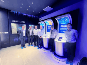
Last week, Dr Christophe Maleville, Chief Technology Officer of Soitec, led a delegation to Singapore to connect with organisations across the local semiconductor ecosystem. The visit covered opportunities in both Silicon Carbide (SiC) and Gallium Nitride (GaN), reflecting Soitec’s interest in engaging with Singapore’s growing capabilities in advanced semiconductor materials and processes.
About Soitec
Soitec is a global leader in the design and production of engineered semiconductor substrates. Their materials are widely used across a range of applications, from consumer electronics to telecommunications and power systems. With a strong presence in both R&D and manufacturing, Soitec works with semiconductor companies and research institutions worldwide to develop substrate solutions that address the evolving needs of the industry.
The Evolving Landscape of Advanced Semiconductor Materials
As global demand for higher efficiency, faster data transmission, and lower power consumption increases, conventional silicon substrates face technical limitations. This has accelerated the industry’s shift toward wide-bandgap semiconductors.
While Silicon Carbide (SiC) continues to revolutionize the power semiconductor space—particularly in electric vehicles and high-voltage grid infrastructure—Gallium Nitride (GaN) has emerged as a critical material for high-frequency applications. Specifically, RF GaN is becoming increasingly vital for the deployment of next-generation telecommunications infrastructure, including 6G networks, advanced radar tracking, and satellite communications.
The Visit to Singapore’s Semiconductor Ecosystem
During their time in Singapore, the delegation met with several research and industry organisations to explore how local innovations align with global technology roadmaps.
As part of their engagement with the local ecosystem, the delegation visited NSTIC (GaN). As a dedicated hub for Gallium Nitride research and development, our center had the opportunity to host the team, showcase our specialized RF GaN work, and highlight our current research capabilities. The visit allowed both teams to engage in technical discussions regarding material performance, processing challenges, and the potential avenues for future collaboration. It was a meaningful exchange and we deeply appreciated the time Dr Maleville and his team took to learn more about the work being done here.
Looking Ahead
It is encouraging to see global semiconductor leaders like Soitec engaging with Singapore’s research community. Cultivating these industry-to-research connections is essential for accelerating the commercialization of next-generation semiconductor technologies. We look forward to continuing the conversation and exploring what a collaborative partnership could look like going forward.
To find out more about NSTIC (GaN) and what we do, get in touch with us. You can also find more in-depth technical papers on our work on our Research Publications page.